What is graphene, and why does it matter?
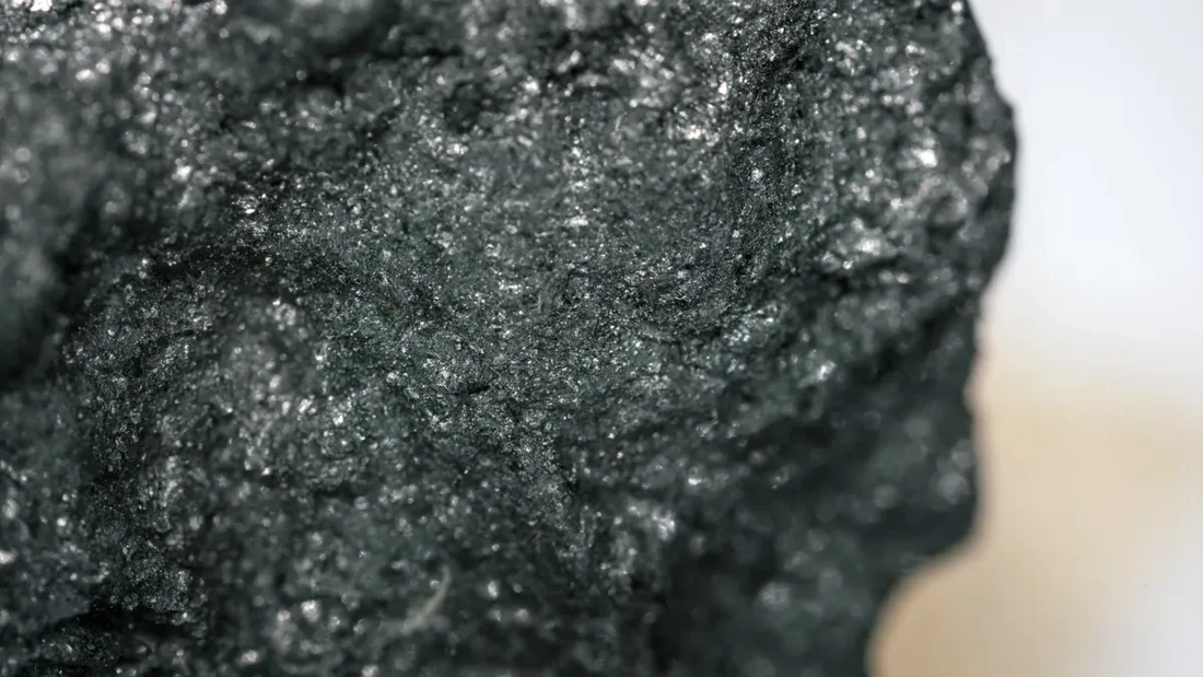
Start with the graphite in a pencil. Follow one carbon sheet through its discovery, remarkable properties, and the practical work of turning a scientific idea into a useful material.
Explore the carbon lattice in 3D
Rotate the model, separate its layers, and isolate one graphene sheet. The illustration uses exaggerated atom sizes and spacing for clarity.
See the bigger picture

Measured properties
97.7%: Visible-light transmission
Approximately 2.3% of incident white light is absorbed by a suspended monolayer. A substrate or coating can change the optical response.
340 N/m: In-plane elastic stiffness
Measured for suspended monolayer membranes. This describes resistance to stretching, not bending, in a two-dimensional sheet.
42 N/m: Intrinsic breaking strength
Reported for a defect-free sheet under the study’s conditions. It is not the strength of every graphene flake, coating or composite.
Production routes
Mechanical exfoliation
Adhesive tape lifts sheets from graphite. This is the peeling idea behind the early graphene experiments. Small flakes for research; placement and large-scale production are difficult.
Liquid-phase exfoliation (LPE)
In this liquid-phase exfoliation (LPE) route, an immersed ultrasonic probe creates cavitation in a graphite suspension, helping separate the layers. The flakes remain dispersed in the liquid. Flakes for inks and mixtures; size, thickness and dispersion need control.
Oxidation and reduction
Chemical treatment adds oxygen-containing groups and helps separate sheets as graphene oxide. Reduction can remove some oxygen to make reduced graphene oxide. Chemically modified material; reduction does not guarantee a pristine honeycomb. Teal dots represent oxygen-containing groups.
Chemical vapour deposition (CVD)
A carbon-containing gas supplies the ingredients for a film to grow on a suitable surface. The film may then be transferred to the surface needed by a device. Continuous films; growth quality, defects and transfer damage matter.
Compressible-flow exfoliation (CFE)
A fast gas stream interacts with layered particles in a nozzle. Gas–sheet interactions can drive sliding and separation of the layers. A route studied for processing layered powders. Gas conditions and particle behaviour matter; the output must be measured to establish its thickness and quality.
What is graphene? A single page from graphite.
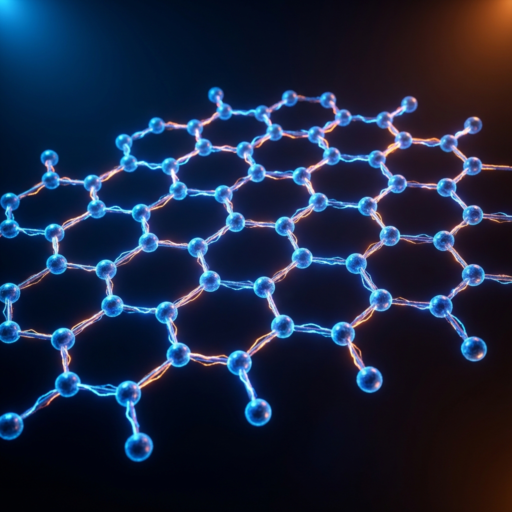
Start with the graphite in a pencil. It looks solid, but inside it are stacks of carbon sheets, like pages in a book. Within each page, carbon atoms are joined in a repeating honeycomb.
Take just one of those pages and you have graphene. The sheet has length and width, but it is only one atom thick. That is why researchers call it two-dimensional, or 2D. It can still bend and ripple.
The three images below follow the journey we are about to take: an everyday material, the structure hidden inside it, and the possibility of putting that structure to work.
SourceThe discovery: making the invisible measurable.
In 2004, Andre Geim and Konstantin Novoselov used adhesive tape to peel graphite into thinner flakes. Among those flakes were sheets just one atom thick. A familiar material could now be investigated one layer at a time.
The breakthrough went beyond peeling a small piece of graphite. Their experiments revealed the unusual behaviour of an isolated sheet, including how it carries electric charge. The work earned them the 2010 Nobel Prize in Physics.
Follow the peeling sequence below, then try the idea with the 3D model. Separate the layers, choose Graphene, and look down on the honeycomb. You have changed the number of sheets while keeping the carbon network.
SourceHow does graphite become graphene?
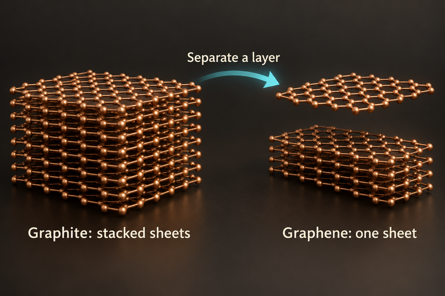
AI-generated teaching illustration; atomic sizes and spacing are illustrative.
Start with a stack
Graphite contains many carbon sheets, one above another.
Separate one sheet
An isolated carbon sheet is graphene. Its atoms are still carbon.
Why is graphene strong, yet flexible?
We have isolated something only one atom thick. Would it tear easily? Picture a fishing net: pulling its edges stretches the connections, while folding it changes its shape. Strong bonds between carbon atoms resist stretching, while the thin sheet can still bend and wrinkle.
Researchers tested graphene by suspending sheets over small openings and pressing them with a tiny probe. They measured elastic stiffness, how strongly a sheet resists stretching, and breaking strength, the load it can withstand before it fails.
Cracks can weaken a real sample, and the measurements depend on the membrane being tested. Still, the first surprise is clear: being thin does not mean being weak.
SourceHow can a sheet be strong and flexible?
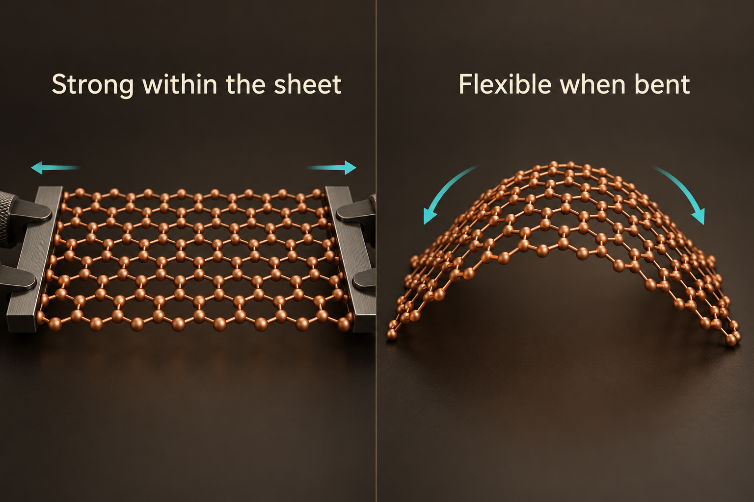
AI-generated teaching illustration; atomic sizes and spacing are illustrative.
Pull along the sheet
Stretching loads the strong bonds between carbon atoms.
Curve the sheet
Bending changes its shape out of the plane. This is a different kind of deformation.
How does graphene carry electricity and heat?
Send an electric current through our sheet. Current is moving charge, and the honeycomb gives electrons unusual ways to move. Ideal single-layer graphene has no conventional band gap: an energy interval separating the electron states called the valence and conduction bands.
SourceThat brings a useful limitation into view. A transistor is an electronic switch, so it must turn current off as well as on. Graphene’s missing conventional gap makes that harder. Carrying charge well is only one part of the job.
SourceNow warm one side. The atoms vibrate, and those vibrations transfer energy through the lattice. Physicists call these vibrational excitations phonons; they carry much of graphene’s heat. A supporting surface or defects in the network can change that flow.
SourceWhat carries electricity, and what carries heat?
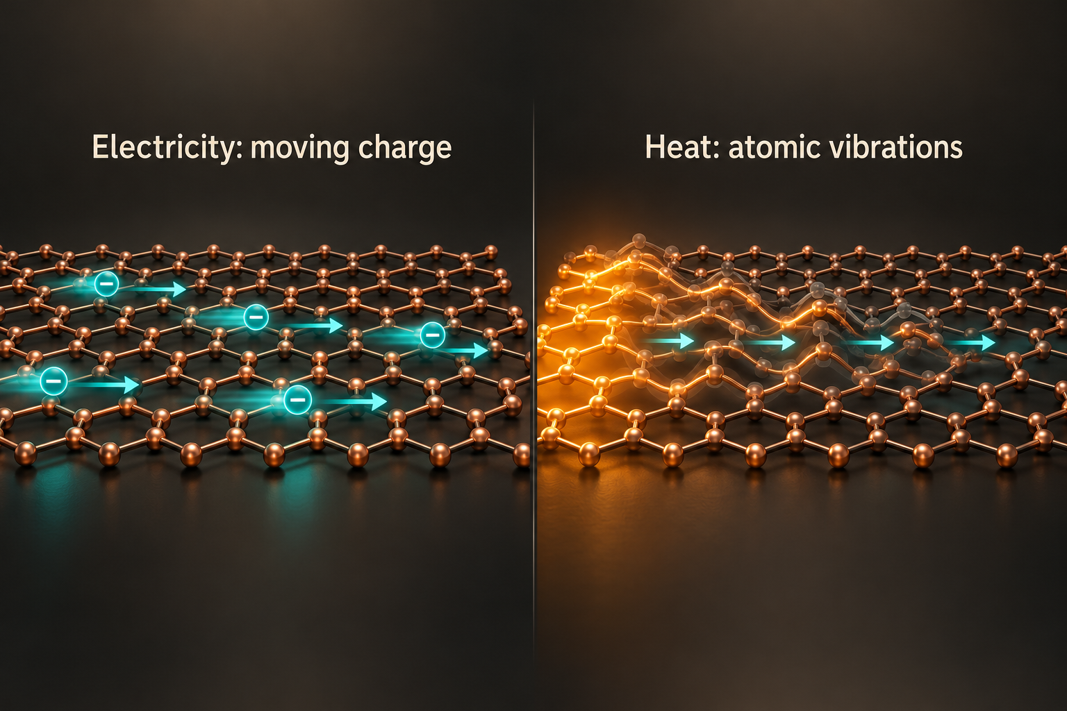
AI-generated teaching illustration; atomic sizes and spacing are illustrative.
Electricity: moving charge
Teal charge symbols show moving carriers; the carbon network remains in place.
Heat: lattice vibrations
The displaced atom positions illustrate vibrations transferring energy through the sheet.
Why is graphene almost transparent?
Hold the same sheet in a beam of light. Most of the light passes through. In experiments on suspended graphene, one layer absorbed about 2.3% of incoming white light, leaving approximately 97.7% transmitted.
Combine that transparency with electrical conduction and you can see why researchers study transparent electrodes: surfaces that make an electrical connection while remaining see-through.
Add sheets with the slider below. Each receives only the light that passed through the previous layer, so the percentages multiply. Layer count is already changing the behaviour of our material.
SourceGraphene, graphite and graphene oxide are different.
The first decision is what we mean by graphene. Our isolated sheet is a monolayer: “mono” means one. Keep a small stack and you have few-layer graphene. A flake is simply a small piece of the material.
SourceChemistry changes the choice too. In graphene oxide, oxygen-containing groups attach to the carbon network. Reduction removes some oxygen, producing reduced graphene oxide, or rGO. It does not automatically restore an ideal clean honeycomb.
SourceThe microscope images below show nitrogen-doped graphene: processed sheets containing nitrogen that changes their properties. Layer count, chemistry and structure all become part of the material we must choose.
SourceWhy are these materials different?
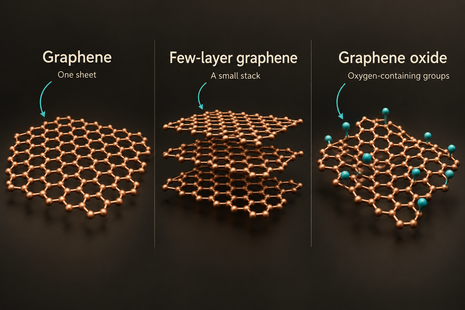
AI-generated teaching illustration; atomic sizes and spacing are illustrative.
Graphene
One carbon sheet.
Few-layer graphene
A small stack of sheets.
Graphene oxide
A chemically modified sheet with oxygen-containing groups.
What processed graphene sheets look like under a microscope
Real sheets can crumple and stack. They do not always look like the perfectly flat honeycomb drawing.
Look at the left image first: the thin material folds and overlaps. The right image zooms in on the layers.
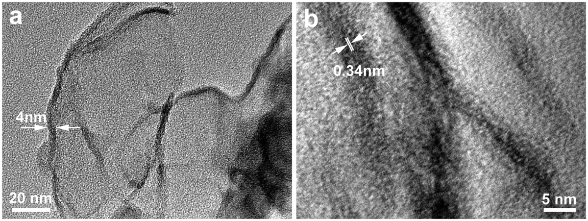
Nitrogen-doped graphene: folded sheets (left) and stacked layers (right).
Panel (a) shows sheet shape; panel (b) shows layer spacing. The scale bars are in nanometres (nm), where one nanometre is one billionth of a metre. The paper describes approximately ten layers in the imaged stack.
Xing, Z., Ju, Z., Zhao, Y. et al. (2016). One-pot hydrothermal synthesis of Nitrogen-doped graphene as high-performance anode materials for lithium ion batteries. Scientific Reports 6, 26146. Figure 3.
Original paper / DOIPublisher figureCC BY 4.0Reproduced without alteration; displayed at a responsive size.
How is graphene made? Choose the route for the job.
Start with the job. A film covering a surface and small flakes mixed into another material require different production routes. Making one remarkable sheet is the beginning of that manufacturing problem.
SourceExfoliation separates layers already present in graphite. Chemical vapour deposition, or CVD, builds a film from carbon supplied through a gas on a suitable supporting surface, called a substrate. The routes below show what each approach does to the carbon.
SourceThe final route connects directly to my research: compressible-flow exfoliation. A fast gas stream can transfer momentum to layered particles, helping sheets slide and separate. That raises a question we can investigate atom by atom: how does the gas make the layers move?
SourceFive routes. What happens to the carbon?
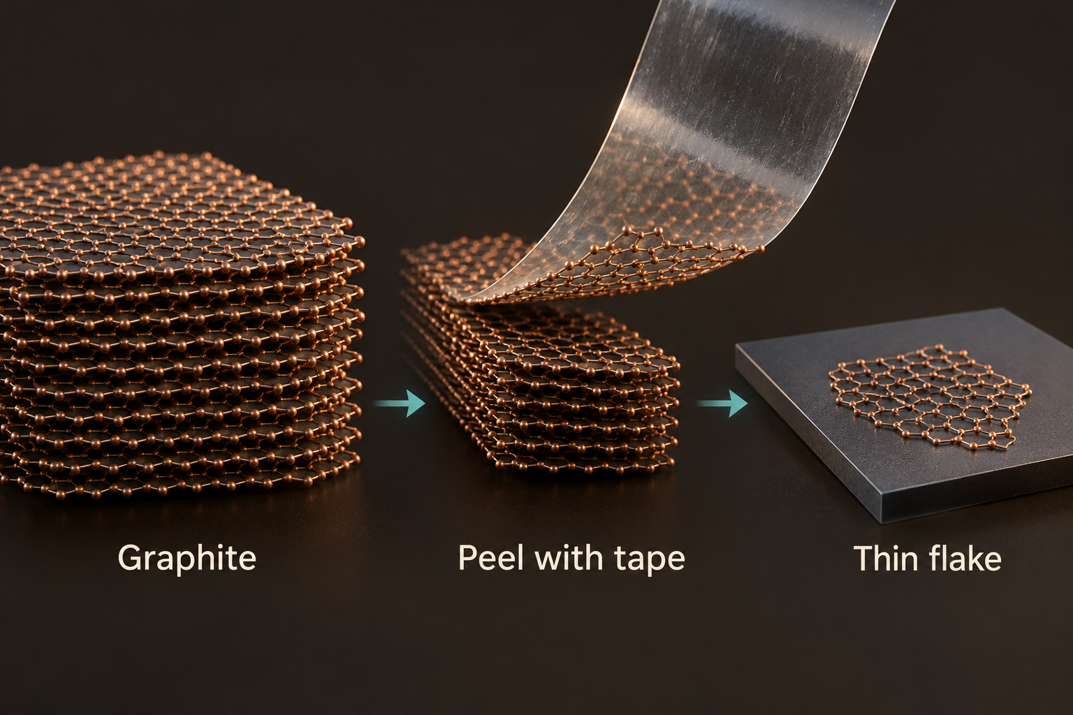
Mechanical exfoliation
Adhesive tape lifts sheets from graphite. This is the peeling idea behind the early graphene experiments.
AI-generated conceptual illustration; not to scale.
Graphite stack → Peel with tape → Thin flake
Small flakes for research; placement and large-scale production are difficult.
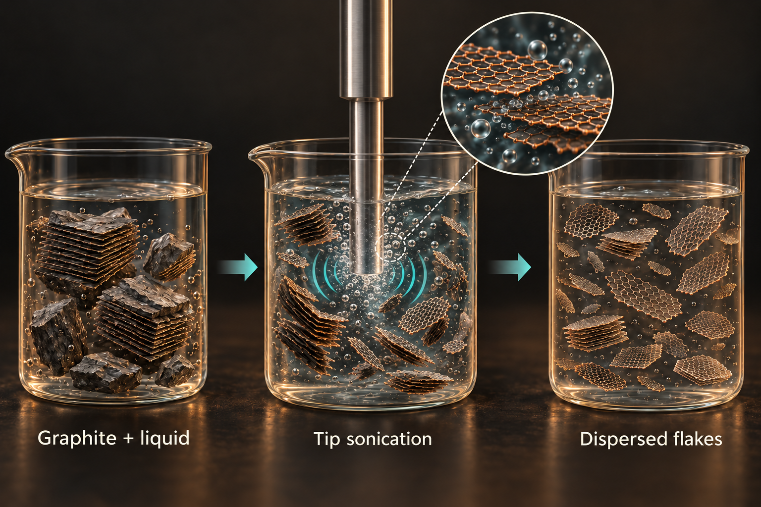
Liquid-phase exfoliation (LPE)
In this liquid-phase exfoliation (LPE) route, an immersed ultrasonic probe creates cavitation in a graphite suspension, helping separate the layers. The flakes remain dispersed in the liquid.
AI-generated conceptual illustration; not to scale.
Graphite + liquid → Tip sonication → Dispersed flakes
Flakes for inks and mixtures; size, thickness and dispersion need control.
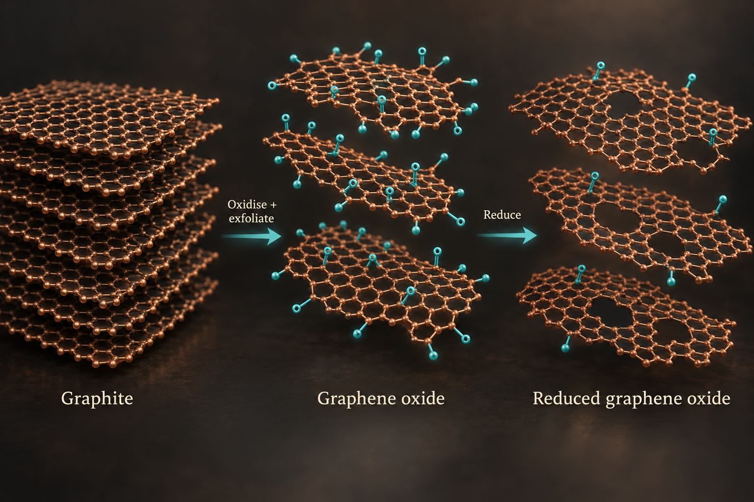
Oxidation and reduction
Chemical treatment adds oxygen-containing groups and helps separate sheets as graphene oxide. Reduction can remove some oxygen to make reduced graphene oxide.
AI-generated conceptual illustration; not to scale.
Graphite → Graphene oxide → Reduced graphene oxide
Chemically modified material; reduction does not guarantee a pristine honeycomb. Teal dots represent oxygen-containing groups.
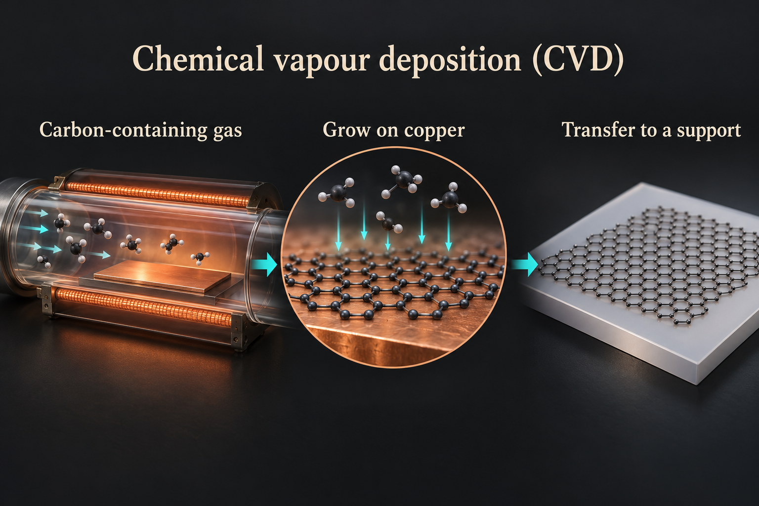
Chemical vapour deposition (CVD)
A carbon-containing gas supplies the ingredients for a film to grow on a suitable surface. The film may then be transferred to the surface needed by a device.
AI-generated conceptual illustration; not to scale.
Carbon feedstock → Grow on a substrate → Transfer / integrate
Continuous films; growth quality, defects and transfer damage matter.
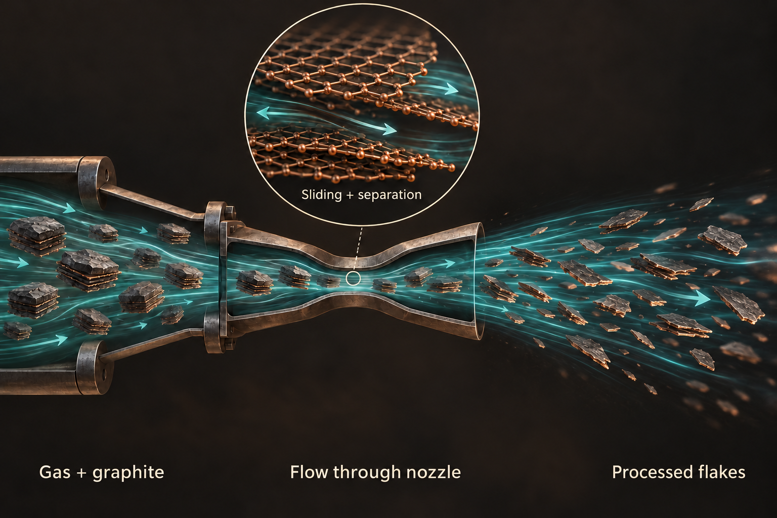
Compressible-flow exfoliation (CFE)
A fast gas stream interacts with layered particles in a nozzle. Gas–sheet interactions can drive sliding and separation of the layers.
AI-generated conceptual illustration; not to scale.
Gas + layered particles → Accelerate through nozzle → Processed flakes
Yield, layer thickness and flake quality still depend on the feedstock and gas conditions. These must be measured for the intended application.
How do researchers know what they have made?
A production route gives us material. A simulation suggests a mechanism. We still need evidence of what was actually made. Shine a laser on the sample: some scattered light exchanges energy with atomic vibrations. Raman spectroscopy measures those energy changes.
SourceFeatures in the spectrum can offer clues about strain, defects and doping. Several effects can alter the same peak, so a single feature is not a complete diagnosis. The question we ask determines which measurements we need.
SourceMicroscopy adds a view of the sheet’s shape and features such as grain boundaries, where regions with different lattice orientations meet. Combining measurements connects the structure we intended to make with the material we have in hand.
SourceHow does Raman spectroscopy work?
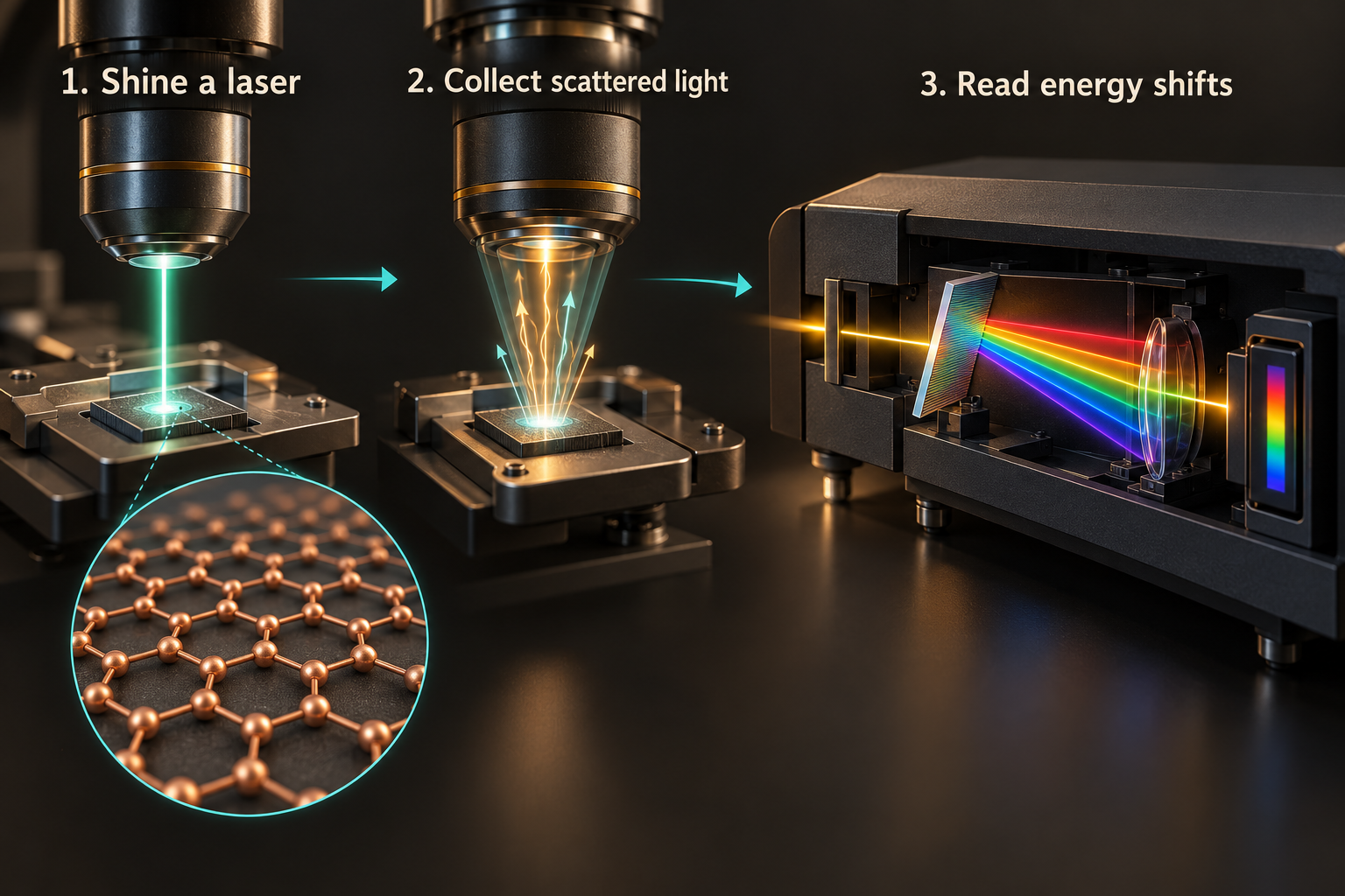
AI-generated teaching illustration; atomic sizes and spacing are illustrative.
1. Shine light
A laser illuminates the graphene sample.
2. Collect scattered light
An instrument measures the light leaving the sample.
3. Read energy changes
Shifts in the light’s energy reveal information about atomic vibrations.
Different measurements tell different parts of the story
Researchers check a chemical change with several measurements, rather than relying on one graph.
Start with the two bottom plots, (c) and (d). The contributions from different carbon–oxygen bonds change after laser treatment.
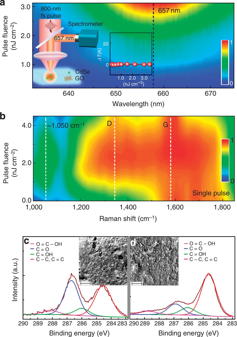
Li and colleagues used light and chemical measurements to study how laser treatment changes graphene oxide. You do not need to interpret every peak to follow the main point: different methods test different parts of the same change.
Panel (a) uses fluorescence, light emitted by a probe, to track temperature. Panel (b) shows Raman measurements of vibrations. Panels (c–d) use X-ray photoelectron spectroscopy (XPS), a method that helps identify chemical bonding by measuring electrons released by X-rays. Small inset images show the surface under an electron microscope.
Li, X., Ren, H., Chen, X. et al. (2015). Athermally photoreduced graphene oxides for three-dimensional holographic images. Nature Communications 6, 6984. Figure 2.
Original paper / DOIPublisher figureCC BY 4.0Reproduced without alteration; displayed at a responsive size.
What is graphene used for, and what still gets in the way?
Our sheet has been separated, tested and measured. Now choose a job for it. A flexible conductor needs a connected film. A composite needs flakes distributed through a host material. The useful form depends on the task.
SourceEach example below connects a property to a material choice and a practical hurdle. The finished system is the test: does it perform better, can it be made consistently, and will it last?
SourceGraphene applications
Sensors: turn a change into a signal
Imagine our sheet as the sensing part of an electronic device. Changes around it can alter its electrical response, giving researchers a signal to measure.
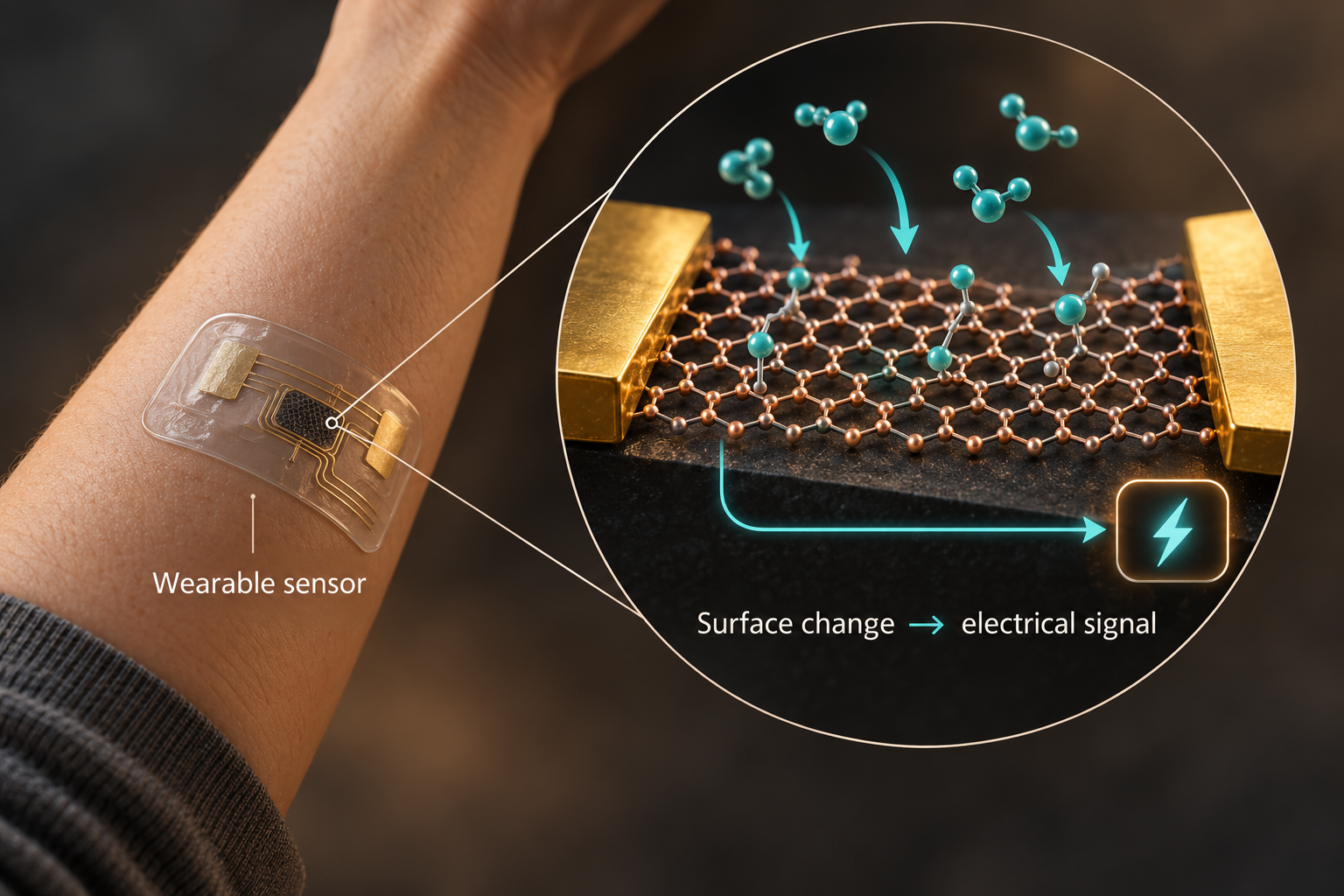
Molecules reaching a specially prepared graphene surface can change its electrical response. The device reads that change as a signal.
Research behind this ideaWhere does it go?
A graphene sheet integrated with electrical contacts.
How can it help?
An exposed surface and an electrical response that can be tuned.
What must work?
A useful sensor must distinguish the intended signal from other changes and remain stable over repeated measurements.
SourceFlexible electronics: conduct while bending
Put a thin conducting layer on a flexible support, and the device can bend with the surface beneath it. Graphene is studied for electronic and optical components where thinness and flexibility matter.
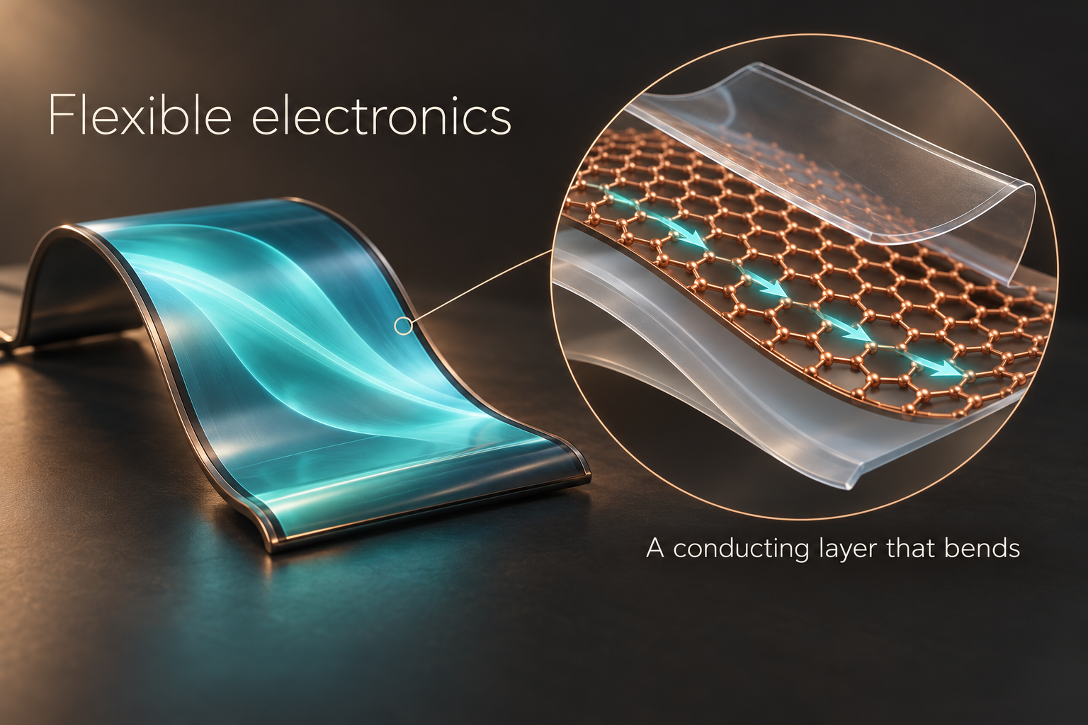
A supported graphene film can carry current while bending with a device. The film is one layer in a larger electronic system.
Research behind this ideaWhere does it go?
A graphene film supported by another material.
How can it help?
Electrical conduction in a thin, flexible layer.
What must work?
Contacts, transfer defects and repeated bending can determine whether the complete device works reliably.
SourceEnergy storage: help the electrode do its job
Inside a battery or supercapacitor, the electrode is where charge is stored or exchanged. Graphene-based materials are explored as parts of those electrodes, often combined with other ingredients.
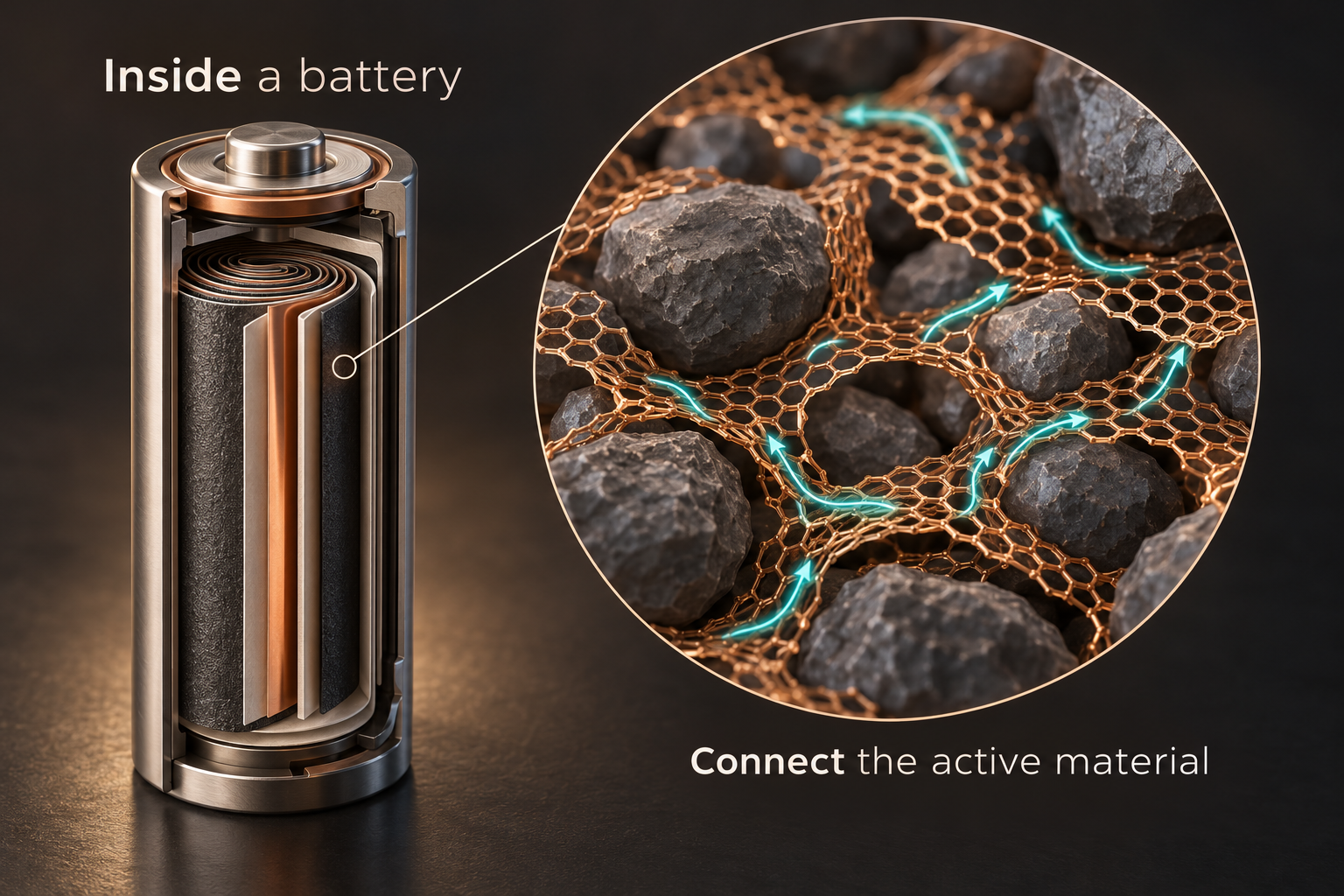
Graphene-containing networks can help connect the particles that store charge. They are part of the electrode, not the whole battery.
Research behind this ideaWhere does it go?
Flakes, porous networks or graphene-containing composites.
How can it help?
Conducting networks and accessible surfaces within an electrode.
What must work?
Measure the whole cell: capacity, charging behaviour, lifetime and manufacturability. Adding graphene alone does not guarantee a better battery.
SourceComposites and coatings: protect a surface
A coating is a thin covering that protects a surface. Adding well-dispersed graphene-related flakes can help make it harder for water or gases to pass through.
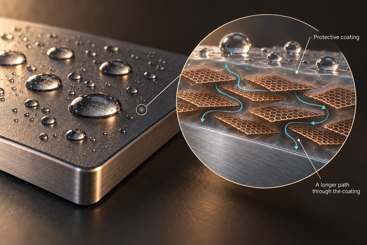
Overlapping flakes can make water or gas take a longer path through a coating. Protection depends on the coating, its defects and how well the flakes are dispersed.
Research behind this ideaWhere does it go?
Graphene-related flakes dispersed in a host material or coating.
How can it help?
Overlapping flakes can create a longer route through a coating.
What must work?
Flakes must be distributed and bonded appropriately. Clumps and weak interfaces can prevent the hoped-for improvement.
SourceThermal management: move heat away
A hot electronic component needs a path for heat to escape. Graphene-based films and composites are investigated as ways to spread that heat across a larger area.
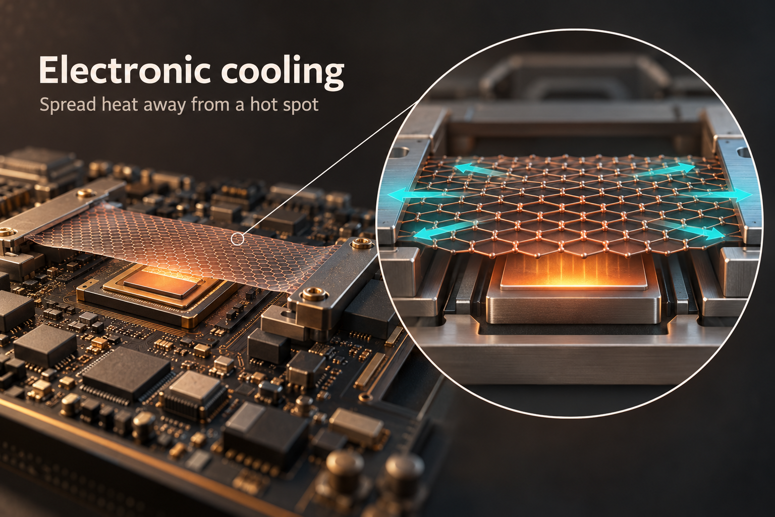
A graphene-based layer can spread heat away from a small hot spot. Other parts of the device must then carry that heat to the surroundings. Layers are shown separated so you can see them; a working heat spreader needs thermal contact with the chip and surrounding assembly.
Research behind this ideaWhere does it go?
A film or composite used as part of a thermal pathway.
How can it help?
Heat transport through the carbon network.
What must work?
Heat must enter and leave the material too. Contact resistance and the surrounding layers can limit the benefit of a highly conducting sheet.
SourceOptics: shape light into an image
Imagine shining light through a carefully patterned film. Researchers have used graphene oxide mixed into a polymer to control that light and reconstruct images with apparent depth.
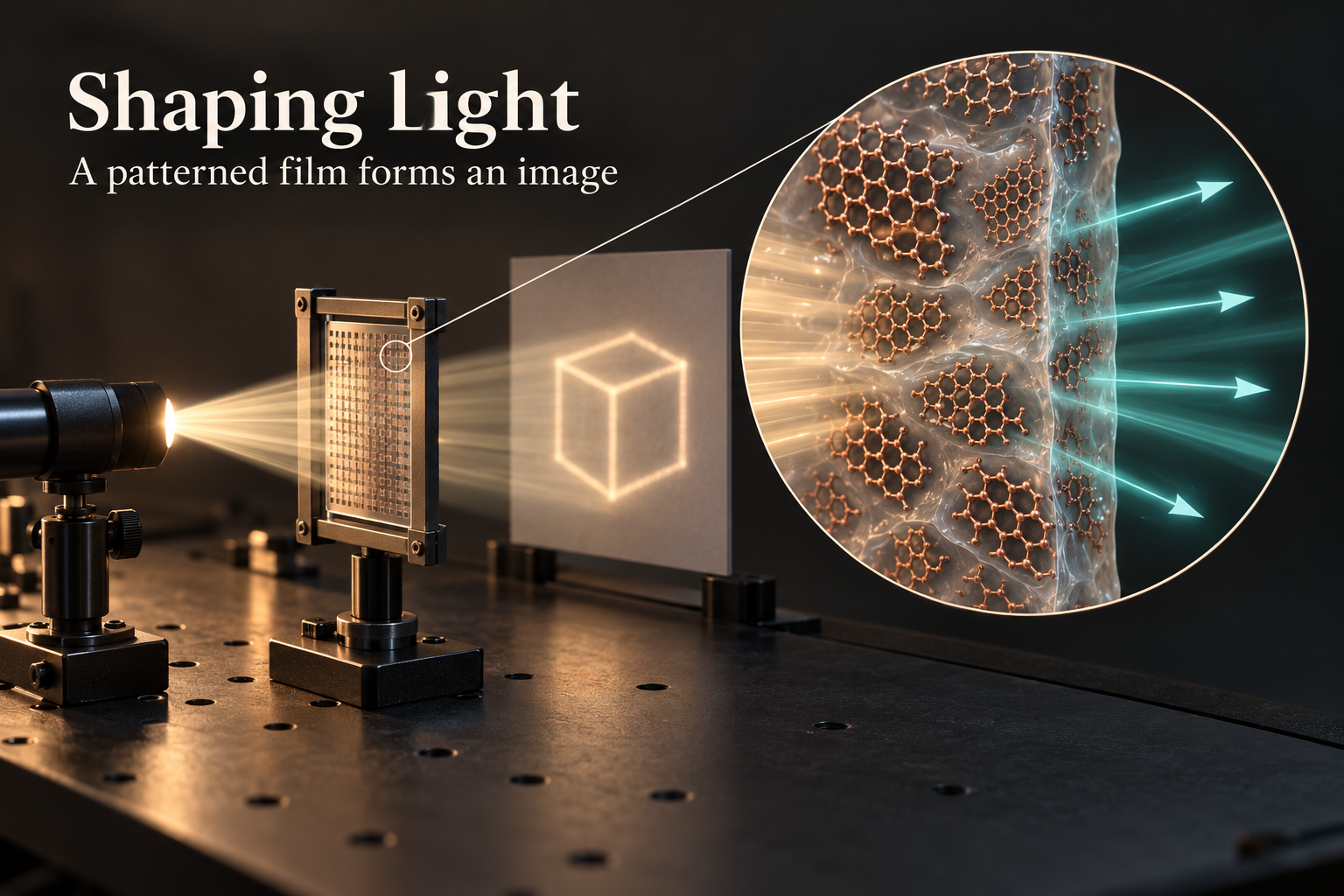
A patterned graphene-oxide composite changes how light passes through it. In research demonstrations, this can reconstruct an image.
Research behind this ideaWhere does it go?
A laser-patterned graphene-oxide polymer composite.
How can it help?
Processing changes the material’s optical response locally.
What must work?
This is a specific laboratory demonstration. Its performance depends on the patterned composite and the optical setup.
SourceKey takeaways
Separate a sheet: graphene is one honeycomb layer of carbon inside graphite.
Follow its structure: bonds, layers, chemistry and defects shape how it behaves.
Give it a job: choose a production route, check the evidence and test the finished system.
Common questions about graphene
What is graphene in simple terms?
Graphene is one layer of carbon atoms arranged in a honeycomb. Stack many such layers and you have the structure of graphite.
Is graphene the same as graphite?
No. Graphene refers to a single carbon sheet; graphite contains stacked sheets. Isolating a layer changes the system and its electronic behaviour.
Can graphene be strong and flexible at the same time?
Yes. Resisting stretching within a sheet and resisting bending are different mechanical properties. The impressive strength measurements describe particular graphene samples, not every graphene-containing product.
Is graphene oxide the same as graphene?
No. Oxygen-containing groups alter graphene oxide’s chemistry and structure. Reduced graphene oxide also differs from an ideal pristine sheet.
Why has graphene not replaced silicon?
Ideal monolayer graphene lacks a conventional semiconductor band gap, making it difficult to turn current off in a logic transistor. Conductivity is only one requirement for an electronic device.
Beyond graphene
Hexagonal boron nitride
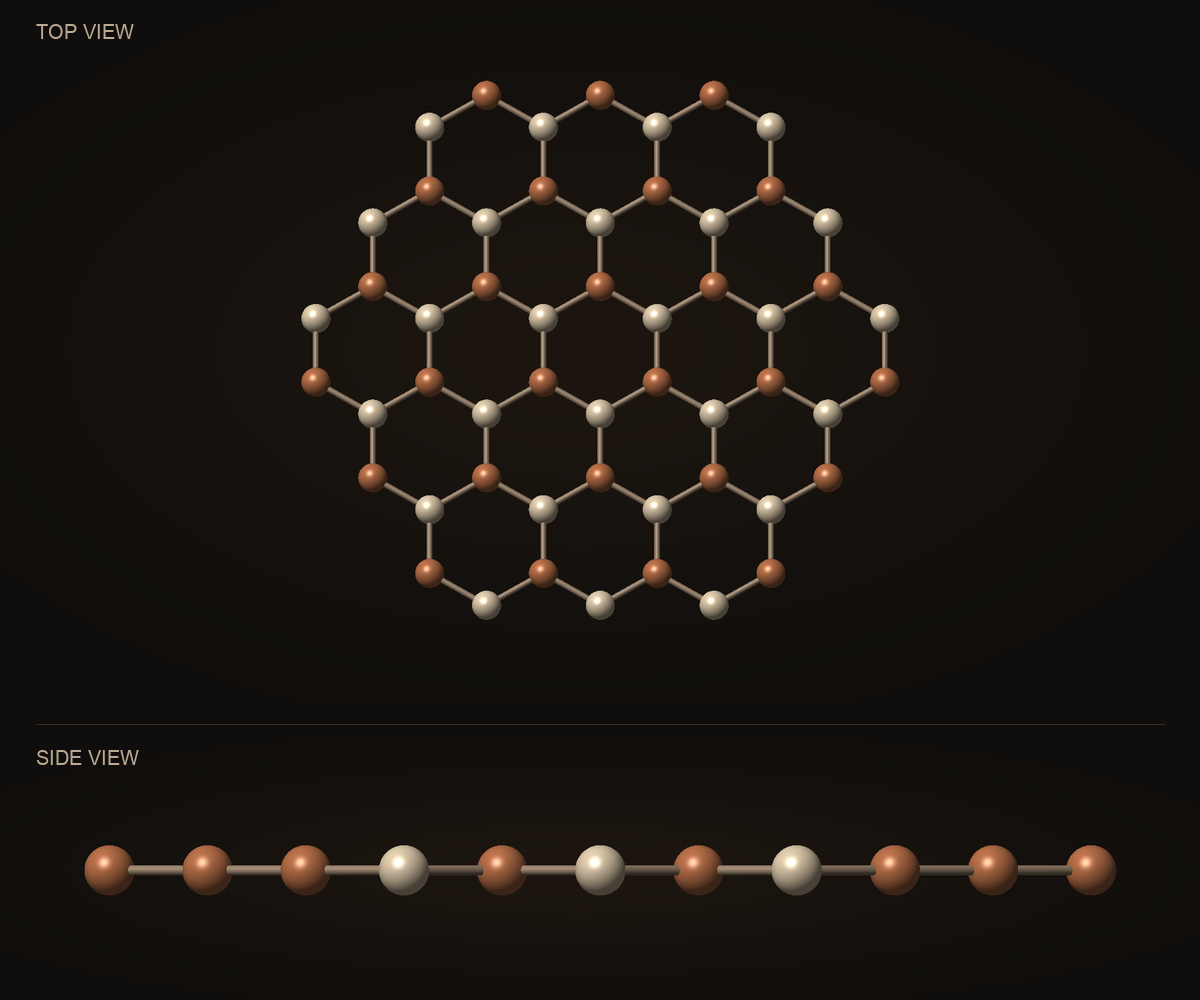
An insulating honeycomb of alternating boron and nitrogen atoms.
SourceMolybdenum disulfide
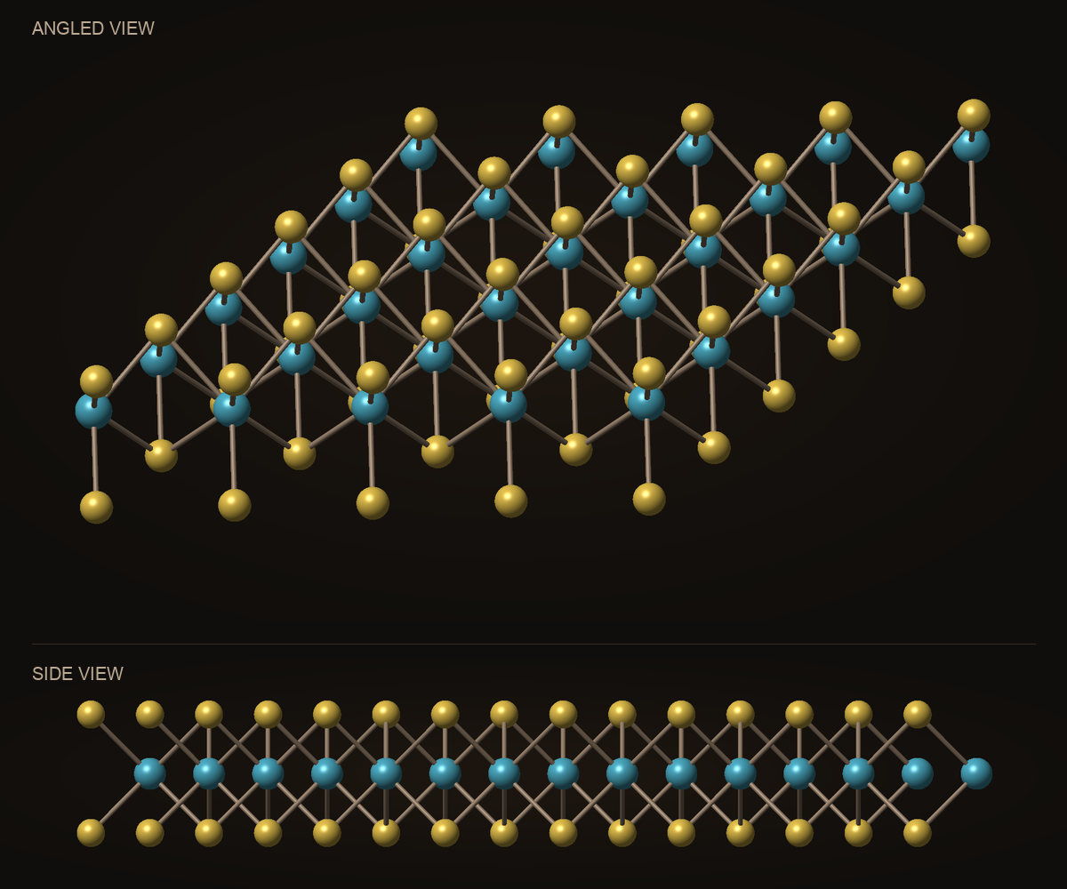
A semiconducting monolayer with molybdenum between two sulfur planes.
SourceMXene
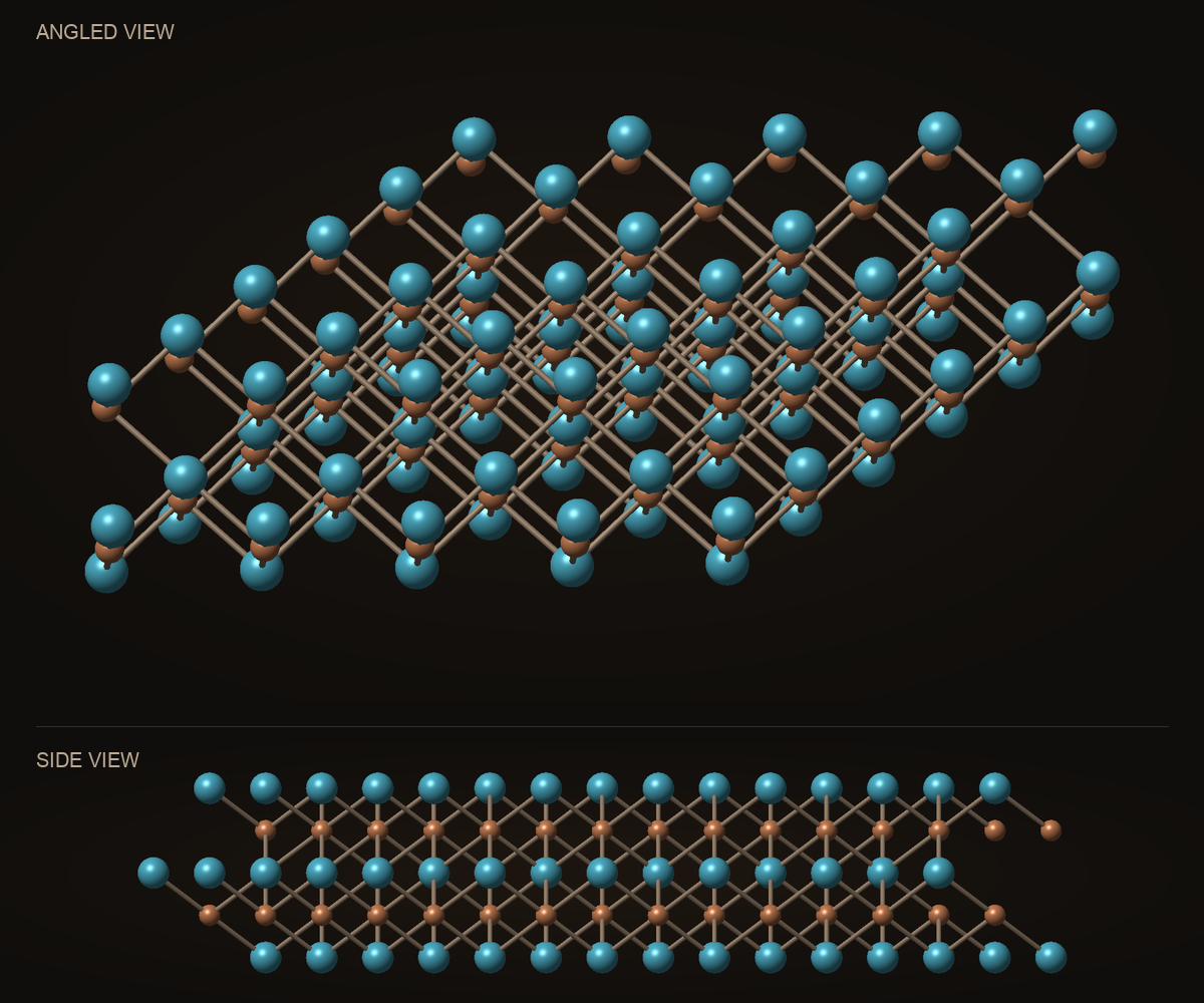
A family of 2D carbides and nitrides. Titanium carbide (Ti₃C₂Tₓ) is one example; surface groups influence its properties.
Source